https://www.tutorialspoint.com/microprocessor/microprocessor_8085_pin_configuration.htm
https://electronicsdesk.com/dma-controller.html
The following image depicts the pin diagram of 8085 Microprocessor −
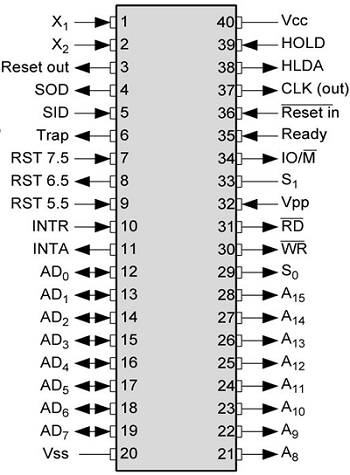
The pins of a 8085 microprocessor can be classified into seven groups −
Address bus
A15-A8, it carries the most significant 8-bits of memory/IO address.
Data bus
AD7-AD0, it carries the least significant 8-bit address and data bus.
Control and status signals
These signals are used to identify the nature of operation. There are 3 control signal and 3 status signals.
Three control signals are RD, WR & ALE.
RD − This signal indicates that the selected IO or memory device is to be read and is ready for accepting data available on the data bus.
WR − This signal indicates that the data on the data bus is to be written into a selected memory or IO location.
ALE − It is a positive going pulse generated when a new operation is started by the microprocessor. When the pulse goes high, it indicates address. When the pulse goes down it indicates data.
Three status signals are IO/M, S0 & S1.
IO/M
This signal is used to differentiate between IO and Memory operations, i.e. when it is high indicates IO operation and when it is low then it indicates memory operation.
S1 & S0
These signals are used to identify the type of current operation.
Power supply
There are 2 power supply signals − VCC & VSS. VCC indicates +5v power supply and VSS indicates ground signal.
Clock signals
There are 3 clock signals, i.e. X1, X2, CLK OUT.
X1, X2 − A crystal (RC, LC N/W) is connected at these two pins and is used to set frequency of the internal clock generator. This frequency is internally divided by 2.
CLK OUT − This signal is used as the system clock for devices connected with the microprocessor.
Interrupts & externally initiated signals
Interrupts are the signals generated by external devices to request the microprocessor to perform a task. There are 5 interrupt signals, i.e. TRAP, RST 7.5, RST 6.5, RST 5.5, and INTR. We will discuss interrupts in detail in interrupts section.
INTA − It is an interrupt acknowledgment signal.
RESET IN − This signal is used to reset the microprocessor by setting the program counter to zero.
RESET OUT − This signal is used to reset all the connected devices when the microprocessor is reset.
READY − This signal indicates that the device is ready to send or receive data. If READY is low, then the CPU has to wait for READY to go high.
HOLD − This signal indicates that another master is requesting the use of the address and data buses.
HLDA (HOLD Acknowledge) − It indicates that the CPU has received the HOLD request and it will relinquish the bus in the next clock cycle. HLDA is set to low after the HOLD signal is removed.
Serial I/O signals
There are 2 serial signals, i.e. SID and SOD and these signals are used for serial communication.
SOD (Serial output data line) − The output SOD is set/reset as specified by the SIM instruction.
SID (Serial input data line) − The data on this line is loaded into accumulator whenever a RIM instruction is executed.
DMA Controller
Definition: DMA or Direct Memory Access Controller is an external device that controls the transfer of data between I/O device and memory without the involvement of the processor. It holds the ability to directly access the main memory for read or write operation.
DMA controller was designed by Intel, to have the fastest data transfer rate with less processor utilization.
We know in order to execute an operation, the microprocessor first fetches the instruction and then decodes it, then further execute it. But individually if the processor is performing all the task inside the system then it unnecessarily keeps the processor busy all the time.
So, to enhance the performance of the processor, an external device is used that can manage data transfer operation between peripherals and memory with least CPU utilization.
Basically, it is nothing but hardware controlled data transfer, where the address and control signals required for transferring the data is generated by an external device. This method of data transfer is known as direct memory access and the external device used for this purpose is known as DMA controller.
Need: We know that generally whenever there exists a need for transfer of data between peripherals and main memory, then first the data is given to the processor by the input device and then the processor further transfers the data to the memory.
And at the time of data transfer operation, the processor cannot be able to execute any other operation.
Hence when the system has a DMA controller then it frees the CPU from data transfer operation and at that particular time being the CPU can execute other operations.
Till now we have discussed the need of DMA controller let us move further and understand how DMA executes any instruction for data transfer.
Operation of DMA Controller in Microprocessor
Basically whenever an I/O device needs to transfer the data to the memory, then it initially sends a request to DMA controller. On receiving data transfer request the controller sends HOLD request to the CPU and waits for HLDA which is nothing but hold acknowledge by the CPU.
So, on getting HOLD request by the controller, the CPU leaves the control over all the buses (i.e., data, control and address bus) and sends HLDA to the controller.
Hence now the processor gets free from any data transfer operation until an interrupt is generated by the DMA controller about the completion of the transfer.
The figure below represents a system having a DMA controller:
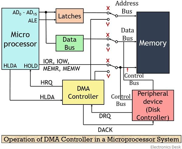
Let us understand the operation of the DMA controller inside the system by considering the idle and active state of the controller.
In the idle cycle of the system, initially when the system gets on, then the processor has control over the system buses, as the switch are connected with the X position.
This is so because, in this position, the buses form the connection between main memory and peripherals through the processor. So, in this position, the processor performs the execution of the instruction.
But once, need arises to read the data from the disk. Then the microprocessor sends an instruction to the disk controller about the read operation of that particular data.
On fetching the required data, the disk controller (peripheral device) sends DMA request, i.e., DRQ signal to the DMA controller. This DRQ signal shows that the device directly wants to transfer the data to the memory without disturbing the processor.
So, on receiving the DRQ signal, HOLD request i.e., HRQ signal is sent by the DMA controller to the microprocessor.
The HRQ signal shows the interest of the DMA controller to have access to system buses. So, on receiving HOLD request, the CPU tristates its buses in order to grant the control to the DMA controller.
Once the processor frees the buses, then it sends the HLDA signal to the DMA controller. And on receiving HLDA signal, the control over the buses is given to the DMA controller as the switch position now changes from X to Y.
So, gaining control over the buses, the active cycle of the DMA gets enabled. Thus now it sends the acknowledge signal DACK to the disk controller that shows that it is now ready for the transfer of data.
Now, after acknowledging the disk controller, further, the DMA controller loads the control signal over the bus according to the operation that is to be performed.
Suppose in case of a write operation, IOR’ and MEMW’ signals are loaded. So, when IOR signal is received by the disk controller then it loads the required data into the data bus. Also, MEMW’ signal shows the presence of address on the address bus where the data is to be transferred.
Thus the disk controller can directly transfer the data to the desired memory location without the CPU utilization.
Once the data transfer is accomplished then the DMA controller generates an interrupt by varying switch position from Y to again X. This indicates the microprocessor about the completion of the data transfer operation.
So, by this, the control of the buses is again transferred to the processor and it starts executing the further operation. This is the basic functioning of the DMA controller inside the system.
Let us have a look at the architectural representation of 8257 DMA controller.
Architecture of 8257 DMA Controller
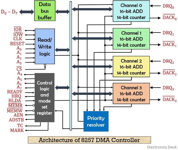
Features of 8257A
- It consists of 4 channels that can be utilized over 4 input/output devices.
- All of the 4 channels can be separately programmed.
- All the 4 channels hold the 16-bit address and 14-bit counters individually.
- The permissible data transfer is up to 64 Kb.
- The operating frequency ranges between 250 Hz to 3 MHz.
- The three operations performed are: read transfer, write transfer and verify the transfer.
- The two operating modes of 8257 are master mode and slave mode.
The figure below shows the pin diagram of 8257 DMA controller: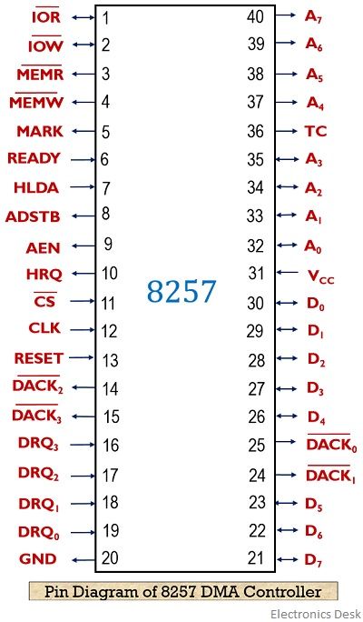
DRQ0 to DRQ3 – Pin number 16 to 19 – These pins get enabled whenever the input device requests the DMA controller for direct data transfer to or from the main memory. Among all the 4, DRQ0 holds the highest priority, in fixed priority mode.
DACK0 to DACK3 – Pin number 14, 15, 24 and 25 – These are active low signals that are nothing but acknowledgement signal generated by the controller to show the acceptance of DMQ by the peripheral devices.
IOR – Pin number 1 – In the master mode of operation, the low signal at this pin indicates the read operation at the peripheral device by the DMA controller. While, in slave mode, it shows that read operation is performed over the internal register by the processor.
IOW – Pin number 2 – It is also an active low pin. A low signal at this pin in master mode shows that write operation is performing over the peripheral device. However, in slave mode, the data bus loads its content at the register.
D0 to D7 – Pin number 26 to 30 and 21 to 23 – These are data lines that hold commands and status words in slave mode. While in the master mode it transfers higher address bytes to the latch.
A0 to A3 – Pin number 32 to 35 – These are 4 least significant address lines that act as input and output in slave and master operating mode of the system respectively.
A4 to A7 – Pin number 37 to 40 – These are basically lower order address lines produced by the controller in master mode.
CLK – Pin number 12 – This pin is used to provide an internal clock frequency signal to 8257.
CS – Pin number 11 – CS denotes chip select and it is an active low pin.
HRQ – Pin number 10 – The enabling of this pin shows the request to directly access the memory by the peripheral device for read-write operation.
HLDA – Pin number 7 – The enabling of this pin represents the acknowledgement by the processor in response to HOLD signal of the DMA controller.
MEMR – Pin number 3 – A low signal at this particular pin represents that read operation is performing over the memory by the peripheral device.
MEMW – Pin number 4 – It is also an active low pin. It gets enabled at the time of memory write operation by the peripheral device.
ADSTB – Pin number 8 – It stands for address strobe. Enabling this pin will demultiplex the address and data bus using latches.
VCC – Pin number 31 – The signal for the operation is applied at this pin.
This is all about the operation of the DMA controller along with 8257 pin description.
No comments:
Post a Comment